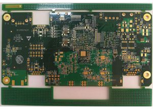
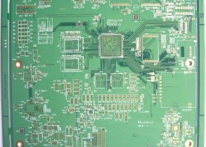
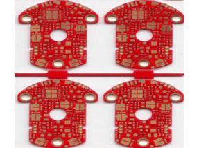
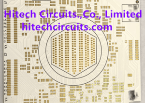
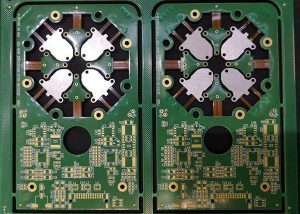
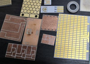
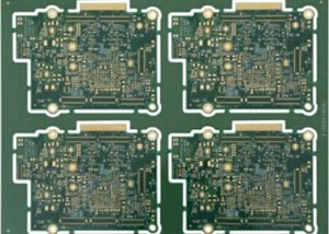
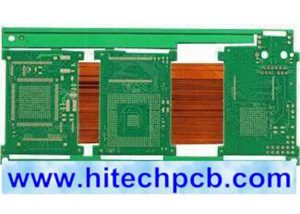
PCB Products
Hitech Circuits is a professional PCB board fabrication, printed circuit board manufacturer, supplier in China, we focus on printed circuit boards manufacturing such as high density interconnect pcb, heavy copper PCB, Power PCB, high frequency pcb, RF PCB, ceramic PCB, Rogers PCB, Teflon PCB and more. If you are looking for a reliable PCB board manufacturer in China, please don’t heisitate to contact [email protected]
What is a PCB?
PCB or Printed Circuit Board is the traditional name for the bare board of which we produce with the layout data and which will be used to mount the components on.
A printed circuit board, or PCB, is used to mechanically support and electrically connect electronic components using conductive pathways, tracks or signal traces etched from copper sheets laminated onto a non-conductive substrate.Components are generally soldered onto the PCB to both electrically connect and mechanically fasten them to it.
Advantages of PCBs
PCBs (printed circuit boards) have, more or less, become a very vital part of modern electronic equipment. In fact, if you were to disintegrate any electronic equipment in your house, the chances are that you are going to come face to face with one of myriad types of PCBs. A basic printed circuit board is comprised of a very large number of passive and active components. They are connected from side to side with traces on the board. It is wholly possible to develop very large circuits on small printed circuits boards with the availability of very small sized electronic components.
But that is not all PCBs are good for. Printed circuit board offer varied advantages which make them the perfect choice for the PCB board manufacturers of electronic components, instruments and equipment everywhere.
Keep on reading to find out what they are.
Compact Size
A characteristic PCB includes a large number of electronic components. Most of these components are very small in size. It would be close to impossible to connect these components together with wires without the aid of printed circuit boards. A typical printed circuit board offers a simple platform to align the electronic components in a compressed and efficient way. This compactness allows creation of big and complicated electronic circuits in small form factors. This, in turn, takes less space in devices.
Ease in Repair and Diagnostic
One great thing about printed circuit boards is that they are helpful in performing diagnostics for a number of reasons. The electronic parts and their polarities on a properly designed printed circuit boards are evidently labeled on the board. This allows convenience during the installation process as well as repair process. Signal paths are often traced during diagnostics. Doing this would be wholly difficult to perform if the traces were not clear to the view and well organized.
Immune to Movement
Another worthwhile thing to notice is that all the components on a PCB are held fixed to the board. This is done by solder flux which does not allow them to move irrespective of the movement of the board itself. Because of this, the electronic circuit (that move or shake) can be placed in devices without worrying about the possibility of displacement of the electronic components and any subsequent electronic short circuits.
Low Electronic Noise
A printed circuit board (that has been properly laid out) lessens electronics noise. If it is not laid out properly then the noise could significantly degrade performance. The electrical components on a printed circuit board are organized in a way that the path lengths of the electrical current between them are lessens. This leads to low radiation and pickup of electromagnetic waves, thus ensuring lower cross talk in between components and in between varied traces, which usually is a major concern in electronic circuits.
Types of Printed Circuit Boards
PCB board fabrication are integral parts of all electronic devices, ranging from simple digital wrist watches and handheld games, to highly complicated satellite systems. PCB are manufactured in several ways to meet the unique requirements of varied industries. They can be fabricated in single sided, double sided, and multi-layered configurations as per the demands.
The following listed are the three basic types of PCB used for several industrial, commercial, and domestic applications.
- Single-Sided – This is the simplest and the most commonly used type of PCB. As the name suggests, these PCB are designed with single substrate. The design of these PCB is such that all copper traces are etched on one side, and the electrical components on the other side of the board. Compared to other types, these PCB are easier to design and fabricate. They are commonly used in calculators, printers, and sensor products, among others.
- Double-Sided – These types of PCB are constructed by mounting electronic components and copper traces on both sides of the substrate. Demands for double sided PCB are on the rise with increasing complexity and density of products. Common applications include control relays, converters, power supplies, power monitoring, and traffic systems.
- Multi-Layered – These types of PCB are characterized by several substrate layers. Each layer is separated from the other by an insulating material. Depending on the complexity of the application, these PCB can be designed with 4, 6, 8, or 10 layers. The layers can even be increased up to 42. Multi-layer PCB are chosen for extremely complicated electronic circuits like central fire alarm systems, fiber optic receptors, nuclear detection systems, and space probe equipment.Having a comprehensive understanding of the basic types of PCB will help you choose the right board for your applications. You can speak to the manufacturer and gain more information pertaining to the pros and cons of each type. Also, you can let your manufacturer know about your requirements; he can suggest the right PCB type that best suits your applications.
Choose the right China PCB manufacturer
PCB or the printed circuit board is certainly one of the most preferred electronic devices today. In keeping with this trend, several companies have come out to manufacturer the PCBs as well. In fact, a few minutes’ search will tell you how numerous this list of manufacturers is. That has certainly one advantage – it has made the market more competitive. But, there are drawbacks as well.
Since there are so many options, you always have the chance of getting confused. So, it is essential that you pick up the right company. Remember, manufacturing Quick turn PCB prototypes is a complex task.
There are plenty of intricate technicalities involved in the entire process. So, you have to be very careful about the quality of the experts who are working on the project. Often, the manufacturers of PCB don’t meet your specific requirements. So, this is another factor that you have to look after.
Finally, finding thePCB manufacturer in Chinafor the small companies has always been a problem. Those big companies out there don’t pay heed to the requirements of the small companies. So, the small companies find it almost compulsory to go to some second grade company and compromise the quality of the PCB.
However, with https://hitechcircuits.com, this problem seems to have come to an end. Their team of dedicated experts put particular importance on the needs of the small companies. At the same time, they ensure the highest quality in their PCBs.
FAQs for Hitech Circuits PCB Products
1. Can Hitech Circuits provide custom PCB solutions? Absolutely! We pride ourselves on our ability to work closely with our clients to design and manufacture custom PCB solutions that meet their specific requirements. Whether you need a unique shape, size, material, or layout, our team of experts is here to help bring your vision to life.
2. What materials are used in your PCBs? Our PCBs are made from a variety of materials to suit different applications and performance requirements. Common materials include FR-4, Aluminum, Copper, Teflon, and more. Each material is chosen for its durability, conductivity, and heat resistance properties.
3. How do you ensure the quality of your PCB products? Quality is our top priority. We adhere to strict quality control processes throughout the manufacturing process, from material selection to final inspection. Our products comply with international quality standards, and we continuously invest in the latest technology and training to enhance our quality assurance practices.
4. What is the lead time for PCB orders? Lead times can vary depending on the complexity and quantity of your order. Generally, standard PCB orders are completed within 2-4 weeks. However, we offer expedited services for urgent projects. Please contact us with your specific requirements for a more accurate estimate.
5. Does Hitech Circuits support low-volume orders? Yes, we understand that not every project requires large quantities of PCBs. We support low-volume orders and offer the same high level of quality and customer service, regardless of order size.
6. Can Hi-Tech Circuits assist with PCB design? While our primary focus is on manufacturing, we can assist with PCB design aspects. We can offer advice on layout, materials, and other technical aspects to ensure your PCB design is optimized for manufacturing and meets your application’s needs.
7. Do you provide after-sales support? Yes, we are committed to providing excellent after-sales support. If you have any questions or issues with your PCBs after delivery, our customer service team is ready to assist you in resolving any problems and ensuring your satisfaction.
8. How does Hi-Tech Circuits contribute to environmental sustainability? We are dedicated to minimizing our environmental impact through various initiatives. This includes using environmentally friendly materials when possible, implementing waste reduction practices, and complying with all relevant environmental regulations. We continually seek ways to improve our environmental performance and reduce the ecological footprint of our products and processes.