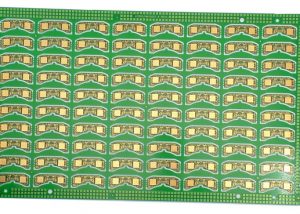
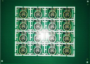
Double Sided PCB
Hitech Circuits Co., Limited is a professional double sided PCB manufacturer engaged in PCB designing and manufacturing, providing the best quality double sided pcb board products, service and the competitive price for our customers. If you need more information about double sided pcb board, two sided printed circuit boards, please don’t hesitate to contact [email protected]
What is double sided pcb ?
The double-layer PCB board with copper on both sides and metallized holes is being called double-layer board. The circuit board on both sides is covered with circuit boards. However, if the wires on both sides want to be used, the appropriate circuit connection between the two sides should be first provided. Today the double sided printed circuit board technology remains the workhorse of the assembly industry. There are near limitless applications for old and new designs.
What materials are used to make double sided PCBs?
The core material is usually fiberglass reinforced epoxy laminate (FR4 is the most common), with copper foil bonded to each side. Other materials may include polyimide, CEM1, and CEM3, depending on the application’s requirements.
Applications of double sided pcb board
- Industrial controls
- Power supplies
- Consumer Electronics
- LED lighting
- Automotive
- Phone systems
- Control relays
- Hard drives
Single vs double sided pcb
The difference between a double-sided PCB board and a single-sided PCB board is that the single-sided PCB circuit is only on one side of the PCB board, while the double-sided PCB circuit can be distributed on both sides of the PCB board. Wiring of the double sided pcb board are being connected.
In addition to the different production process between double-sided PCB board and single-sided PCB board, there is an additional copper sinking process, which is the process of conducting double-sided circuits.
Are Double Sided PCBs more expensive than Single Sided PCBs?
Generally, yes. The manufacturing process for Double Sided PCBs is more complex, involving additional steps such as through-hole plating. This complexity can lead to a higher cost compared to Single Sided PCBs.
Can double sided PCBs be used in high-frequency applications?
Yes, Double Sided PCBs can be used in high-frequency applications. The key is in the material used for the PCB substrate and the precision of the layout. High-frequency PCBs often require materials with low dielectric losses and a design that minimizes signal interference, which can be achieved with careful planning and expertise in double-sided PCB design.
Advantages of double sided pcb
- Double sided pcb make it relatively easy to add conductive paths on the board, which means you will have a PCB that better suits your needs;
- Since both sides of double-sided pcb board are conductive, a large number of ICs and components can be assembled at any time;
- If necessary, the size of the circuit board can be reduced, because double-sided can be used, this type of PCB may save you money because you may only need to use one board;
- Double-sided PCB can be used in many different applications and electronic products, double-sided PCB is ideal for demanding applications and advanced electronic products.
Disadvantages of double sided pcb
- When conducting large currents, double-sided printed circuit boards are not ideal because the copper wires are heated. We are aware of this and ensure that all PCBs are of high quality and are not damaged.
- When soldering double sided PCB, there is a risk of overheating. However, our PCB experts have manufactured thousand kinds of PCBs and know how to minimize risks.
- Double sided pcb boards can be very complex, which means they can be difficult to manufacture. The good news is that Hitech has extensive experience in manufacturing various double-sided PCBs. You can count on us to get the job done.
How to solder double sided pcb
In order to ensure reliable electrical conduction of the double-sided printed circuit board, the connection holes on the double-sided pcb board (that is, the through-hole part of the metallization process) should be welded first with wires or the like, and the protruding part of the connecting wire tip should be cut to avoid stabs Injury to the operator’s hand, this is the preparation work for the wiring of the board.
The essentials of double-sided circuit board soldering:
- For devices that require shaping, they should be processed according to the requirements of the process drawings; that is, they must be shaped first and then plug-in.
- After shaping, the model side of the diode should face up, and there should be no discrepancies in the length of the two pins.
- When inserting devices with polarity requirements, pay attention to their polarity not to be reversed. Roll integrated block components, after inserting, no matter it is a vertical or horizontal device, there must be no obvious tilt.
- The power of the soldering iron used for soldering is between 25~40 wattages. The temperature of the soldering iron tip should be controlled at about 242℃. If the temperature is too high, the tip is easy to “die”, and the solder cannot be melted if the temperature is low. The soldering time should be controlled at 3~4 seconds.
- During the formal welding, generally operate according to the welding principle of the device from short to high and from the inside to outer. The welding time should be mastered. If the time is too long, the device will be burnt, and the copper line on the copper clad board will also be burnt.
- Because it is double-sided welding, a process frame or the like for placing the circuit board should also be made, so as not to squeeze the components underneath.
- After the circuit board welding is completed, a comprehensive check-in check should be carried out to find out where there is missing insertion and soldering. After confirmation, trim the redundant device pins and the like on the circuit board, and then flow into the next process.
- In the specific operation, the relevant process standards should be strictly followed to ensure the welding quality of the product.
How to reflow double sided pcb
At present, the mainstream circuit board assembly technology in the SMT industry should be reflow soldering. Of course, there are other circuit board soldering methods. Double-sided reflow can save the space of the circuit board, which means that smaller product can be achieved, so most of the double sided pcb boards seen on the market belong to the double-sided reflow process.
Because the double-sided reflow process requires two reflows, there are some process limitations. The most common problem is that when the pcb board goes to the second reflow furnace, the parts on the first side will be affected by gravity and dropped, especially when the board flows to the reflow zone of the furnace at high temperature, below we will explain the precautions for the placement of parts in the double-sided reflow process:
Firstly, smaller parts are recommended to be placed on the first side to pass through the reflow oven, because the deformation of the PCB will be smaller when the first side passes through the reflow oven, and the precision of solder paste printing will be higher, so it is more suitable to place smaller parts.
Secondly, the smaller parts will not be at risk of falling during the second pass through the reflow oven. Because the parts on the first side are placed directly on the bottom side of the circuit board when hitting the second side, when the board enters the reflow area, it will not fall off the board due to excessive weight.
Thirdly, the parts on the first side must go through the reflow oven twice, so its temperature resistance must be able to withstand the temperature of two reflows. The general resistance and capacitor are usually required to pass the high temperature of at least three reflows. This is to meet the requirements that some boards may need to go through the reflow furnace again due to maintenance.
FAQs for Double-Sided PCBs at Hitech Circuits
- Can Hi-Tech Circuits customize Double-Sided PCBs? Absolutely! We offer custom PCB design and manufacturing services to meet your specific requirements. Whether you need unique shapes, sizes, or specific electronic components, we can accommodate your needs.
- What is the lead time for Double-Sided PCB orders? Lead times can vary depending on the complexity and quantity of your order. Generally, our lead times range from 5 to 15 working days. For more precise estimates, please contact our customer service.
- Do you offer prototyping services for Double-Sided PCBs? Yes, we do! Prototyping is an essential step in the PCB development process, allowing you to test and refine your design before moving to mass production. We offer quick and cost-effective prototyping services.
- How do you ensure the quality of your Double-Sided PCBs? We adhere to strict quality control standards throughout the manufacturing process, including inspection of raw materials, in-process inspection, and final testing. Our commitment to quality ensures that you receive reliable and durable PCBs.
- Can Hi-Tech Circuits assist with PCB layout and design? Yes, our team of experienced engineers can assist with PCB layout and design, ensuring your PCB meets all electrical and mechanical requirements for optimal performance.
- What file formats do you accept for Double-Sided PCB designs? We accept various file formats, including Gerber files, Eagle, Altium, and KiCad. If you have another format, please contact us, and we’ll do our best to accommodate your needs.