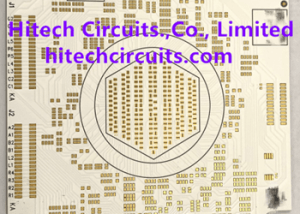
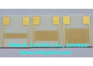
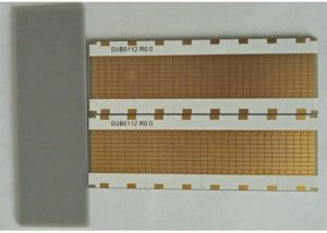
Ceramic PCB
We are a professional ceramic pcb manufacturer, supplier from China, we mainly supply high quality Alumina (Al2O3) Ceramic PCB, Aluminum Nitride (AIN) Ceramic PCB board and IGBT Ceramic PCB. Our ceramic printed circuit boards features of high pressure, high insulation, high temperature, and high reliable and minor volume electronic products, Hitech is your best choice for ceramic PCB boards and needs.
What is ceramic pcb board
Ceramic pcb boards are actually made of electronic ceramics as the basic material and can be made in various shapes. Among them, the characteristics of high temperature resistance and high electrical insulation of ceramic circuit boards are the most prominent. The advantages of low dielectric constant and dielectric loss, high thermal conductivity, good chemical stability, and similar thermal expansion coefficient to components are also very significant.
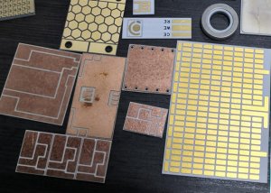
Different types of ceramic pcb
Ceramic PCB is widely used in power electronics, electronic packaging, hybrid microelectronics and multi-chip modules due to its excellent thermal conductivity and air tightness. But not everyone is clear about the classification. Many manufacturers think ceramic PCBs are expensive and fragile as soon as they hear about ceramic PCBs. Yes, this is indeed a shortcoming of ceramic PCBs, but not all ceramic PCBs are like this. Today we will tell you about the different types of ceramic PCBs.
Al2O3 ceramic PCB
Al2O3 ceramic PCB ( alumina ceramic PCB) refers to various ceramic PCBs with Al2O3 as the main raw material and an Al2O3 content of more than 75%. It has a rich source of raw materials, with advantages of low price, high mechanical strength and hardness, good insulation performance, good heat shock resistance, good chemical resistance, high dimensional accuracy, and good adhesion to metals. It is a ceramic substrate material with good comprehensive performance. Currently used Al2O3 ceramic substrates, the content of Al2O3 accounts for 85% to 99.5%. Among them, 96% Al2O3 ceramic PCB is widely used in the production of thick film circuit substrates and chip devices. The thermal conductivity of Al2O3 at room temperature is 29W/(m·K), which is close to the thermal conductivity of steel; with the increase of Al2O3 content, the electrical insulation performance and thermal conductivity of Al2O3 ceramic PCB will increase, but At the same time, it will also lead to an increase in the firing temperature, an increase in energy consumption, a large loss of kiln furniture, and an increase in manufacturing costs.
SiC ceramic PCB
The thermal conductivity of SiC ceramic PCB is very high, 100~490W/(m·K) at room temperature, and it is related to the purity of SiC crystals. The higher the purity, the greater the thermal conductivity; the oxidation resistance is good, and the decomposition temperature is above 2500℃, it can still be used at 1600℃ in an oxidizing atmosphere; the coefficient of thermal expansion is also low, and it is close to Si, with good electrical insulation performance; SiC has a Mohs hardness of 9.75, second only to diamond and cubic BN, and has high mechanical strength. SiC ceramics have strong covalent bond characteristics and are difficult to sinter. Usually, a small amount of boron or aluminum oxide is added as a sintering aid to increase the density. Experiments show that beryllium, boron, aluminum and their compounds are the most effective additives, which can make SiC ceramics denser than 98%.
BeO ceramic PCB
BeO has a brazine structure, in which oxygen ions are arranged in a hexagonal close-packed manner to form a hexagonal lattice. The general oxide is usually an ionic compound, but BeO has a strong covalent bond and an average molecular weight of only 12. Because of its good electrical properties, luminescence and photochemical properties, high mechanical strength, low dielectric loss, etc, it become one of the materials that people pay attention to.
AlN ceramic PCB
AlN ceramic PCB (aluminum nitride ceramic) is a new type of high thermal conductivity ceramic packaging material. It has been extensively studied in the 1990s and gradually developed. It is currently generally considered to be a promising electronic ceramic packaging PCB. AlN material has high thermal conductivity, excellent dielectric properties, high electrical insulation strength, stable chemical properties, strong corrosion resistance, and good mechanical properties. In particular, its thermal expansion coefficient matches with silicon, which makes it an ideal semiconductor packaging substrate materials and have been widely used in integrated circuits, microwave power devices, millimeter-wave packaging, high-temperature electronic packaging and other fields.
Ceramic PCB for IGBT Module
IGBT stands for insulated-gate bipolar transistor. It is a bipolar transistor with an insulated gate terminal. The IGBT combines, in a single device, a control input with a MOS structure and a bipolar power transistor that acts as an output switch. IGBTs Ceramic PCB are suitable for high-voltage, high-current applications. They are designed to drive high-power applications with a low-power input.
IGBT, or Insulated Gate Bipolar Transistor, is a BJT transistor with a MOS Gate, or we can say an IGBT module is the combination of a BJT and a MOS Gate. An IGBT chip is small in size, but it can control electrical energy transmission and achieve 100,000 times of current switch at ultra-high voltages of 650 million V in only 1 second.
IGBT modules have been applied in automotive, industrial, aerospace, consumer electronics, and many other industries for many years. But how to optimize the thermal dissipation of an IGBT package so the module can work at a higher power? If thermal can dissipate more quickly, the IGBT module can have more advanced applications. For this purpose, engineers are using ceramic PCBs for IGBT packaging.
Ceramic PCBs dissipate thermal from IGBT chip to the outer packaging
You may ask, how much thermal does an IGBT module generate when it works? It is equal to the heat generated by 100 electric furnaces. So much thermal has to be dissipated immediately from the IGBT chip and leads to the application of ceramic PCBs.
How does a ceramic PCB protect the IGBT module from the heat? In an IGBT module, a ceramic PCB is placed under the IGBT chip, or we can say that the chip is assembled on the ceramic circuit board. The ceramic PCB connects and supports the chip and dissipates thermal quickly from it to the outer packaging. In this way, the chip is protected from the influence of thermal.
Why Ceramic PCBs can be used for IGBT thermal dissipation
There are alumina (Al₂O₃) PCBs, aluminum nitride (AlN) PCBs, and silicon nitride (Si₃N₄) PCBs used for thermal dissipation of IGBT modules.
Why ceramic PCBs can dissipate thermal effectively for the IGBT module? Because ceramic materials have good properties of thermal dissipation and electrical insulation. Unlike aluminum substrate PCBs, ceramic PCBs do not use an insulation layer that hinders thermal dissipation. During the ceramic PCB manufacturing process, the copper-clad is directly bonded onto the ceramic substrate at high temperatures under high pressures. Then the circuit layer is manufactured by the photoresist coating method. When the circuit board is manufactured, the IGBT and other components are mounted on the board. Ceramic materials have ultra-high insulation and can withstand breakdown voltage up to 20KV/mm. The thermal conductivity of alumina PCBs is 15-35W/mK, aluminum nitride PCB 170-230W/mK, and silicon nitride PCB 80+W/mK. On the contrary, an aluminum PCB has thermal dissipation of only 1-12W/mK.
Usages and applications of ceramic printed circuit boards
Ceramic printed circuit boards have a wide range of applications and can be used in the LED field, solar panel components, high-power power semiconductor modules, semiconductor refrigerators, electronic heaters, power control circuits, power hybrid circuits, smart power components, high-frequency switching power supplies , solid state relays, automotive electronics, communications, aerospace and military electronic components.
Advantages of ceramic PCB boards
- Higher thermal conductivity
- More matching thermal expansion coefficient
- Stronger and lower resistance metal film
- The solderability of the substrate is good, and the use temperature is high
- Good insulation
- Low high frequency loss
- High-density assembly is possible
- It does not contain organic ingredients, is resistant to cosmic rays, has high reliability in aerospace and has a long service life
- The copper layer does not contain an oxide layer and can be used for a long time in a reducing atmosphere
Disadvantages of ceramic pcb boards
1. Fragile
This is one of the most important shortcomings. At present, only small-area ceramic printed circuit boards can be produced.
2. Expensive
There are more and more requirements for electronic products. Ceramic circuit boards only meet the requirements of some relatively high-end products, and low-end products will not be used at all.
Ceramic PCB VS Aluminum PCB
The biggest difference between the ceramic PCB and the aluminum PCB is the material and structure. The ceramic PCB uses ceramic as the substrate material. In terms of structure, the insulation performance of the ceramic itself is very good, so the ceramic PCB does not need an insulating layer.
The aluminum PCB is a metal-based copper clad laminate with good heat dissipation function. Generally, a single side pcb is composed of a three-layer structure, which is a circuit layer (copper foil), an insulating layer and a metal base layer. For high-end use, it is also designed as a double-sided PCB board, and the structure is circuit layer, insulating layer, aluminum base, insulating layer, and circuit layer. Very few applications are using multi-layer boards, which can be formed by bonding ordinary multi-layer pcb boards with insulating layers and aluminum bases.
The thermal conductivity of the aluminum PCB is almost between 1.0 and 2.0. It can be seen from the structure that the aluminum PCB has an insulating layer, so its thermal conductivity is mainly related to the insulating layer. The thermal conductivity of the aluminum PCB with an insulating layer is not outstanding, but much better than the general FR-4 PCB.
At present, the ceramic PCBs on the market are mainly aluminum nitride ceramics and alumina ceramics. The thermal conductivity of alumina ceramics is almost 15~31, and the thermal conductivity of aluminum nitride is almost 135~175.
Obviously, the thermal conductivity of ceramic PCB is much better than that of aluminum PCB. The insulating layer is the core technology of aluminum PCB, which mainly plays the role of bonding, insulation and heat conduction. The insulating layer of the aluminum PCB is the largest thermal barrier in the power module structure. The better the thermal conductivity of the insulating layer, the more conducive to the diffusion of heat generated during the operation of the device, and the more conducive to reducing the operating temperature of the device, so as to achieve the purpose of increasing the power load of the module, reducing the volume, extending the life, and improving the power output. In other words, the aluminum PCB performance is subject to the insulating layer. The ceramic PCB has no insulating layer, so there will be no such troubles.
Main manufacturing process of ceramic pcb
- Drilling: the use of mechanical drilling to produce connecting pipes between metal layers
- Plated through holes: After the copper lines between the connecting layers are drilled, the circuits between the layers are not conductive. Therefore, a conductive layer must be formed on the hole wall to connect the lines. This process is generally called “PTH Process” in the industry. The main working procedures include three procedures of slag removal, chemical copper and copper electroplating.
- Dry film lamination: production of photosensitive etching resistive layer.
- Inner circuit image transfer: Use exposure to transfer the image of the negative to the board surface.
- Outer circuit exposure: After the photosensitive film is attached, the circuit board has gone through a manufacturing procedure similar to that of the inner circuit board, and then exposed and developed again. The main function of the photosensitive film this time is to define the areas that need electroplating and those that do not need electroplating, and the area we cover is the area that does not need electroplating.
- Magnetron sputtering: Using the energy and momentum exchange between the positive ions generated in the gas glow discharge process and the surface atoms of the target material, the material is moved from the source material to the substrate to realize the deposition of the thin film.
- Etching – Formation of external circuits: A technology that removes materials using chemical reaction or physical impact. The functionality of etching is reflected in the selective removal of specific patterns. After the electroplating of the circuit is completed, the circuit board will be sent for stripping, etching, and stripping the tin wire. The main work is to completely strip the electroplating resist and expose the copper to be etched in the etching solution. Since the top of the circuit area has been protected by tin, an alkaline etching solution is used to etch the copper, but because the circuit has been protected by tin, the circuit in the circuit area can be retained, so that the surface circuit of the overall circuit board appears.
- Solder-resistant paint coating: The purpose of ceramic circuit boards is to carry electronic parts and achieve the purpose of connection. Therefore, after the circuit of circuit board is completed, the area where the electronic parts are assembled must be defined, and the non-assembly area should be properly protected with polymer materials. Since solder is used for the assembly and connection of electronic parts, this kind of polymer material that partially protects the circuit board is called “solder resist paint.” At present, most photosensitive solder resists paint use wet ink coating.
Preparation process and technology of ceramic PCB
The preparation process of ceramic PCB can be divided into four categories: HTCC, LTCC, DBC and DPC.
- HTCC (High-Temperature Co-fired Ceramic) preparation method requires a temperature above 1300°C, but due to the choice of electrode, the preparation cost is quite expensive;
- The preparation of LTCC (Low-Temperature Co-fired Ceramic) requires a calcination process at about 850°C, but the precision of the prepared circuit is poor, and the thermal conductivity of the finished product is low;
- The preparation method of DBC (Direct Bonded Ceramic) requires the formation of an alloy between copper foil and ceramics, and the calcination temperature needs to be strictly controlled within the temperature range of 1065-1085°C. Because the preparation method of DBC requires the thickness of copper foil, it should generally not be lower than 150~300 microns, thus limiting the wire width to depth ratio of this type of ceramic circuit board.
- The preparation method of DPC (Direct Plated Ceramic) includes vacuum coating, wet coating, exposure and development, etching and other process, so the price of its products is relatively high. In addition, in terms of shape processing, DPC ceramic PCB need to be laser cut, traditional drilling, milling machines and punching machines cannot accurately process them, so the bonding force and line width are more precise with laser cutting.
Advantages of Ceramic PCB
As the name implies, a ceramic PCB is a circuit board using ceramic as a substrate. The performance of ceramics is better than that of ordinary substrates. It is a circuit board prepared by using a thermally conductive ceramic powder and an organic binder at a temperature lower than 250 °C, and its thermal conductivity is 9-20 W / m.k. Ceramic circuit boards are widely used in the manufacture of the electronics industry. Due to their advantages of good thermal conductivity, high voltage resistance, and stable chemical properties, ceramic circuit boards have become an important component in the manufacture and manufacture of electronic products.
Thermal conductivity refers to the ability of a substrate to transfer heat energy. The higher the conductivity, the better the thermal conductivity. So heat energy can be effectively transferred to the heat dissipation system, which reduces the temperature of the product and extends the life of the product. Since the main material of the ceramic PCB is ceramic, and the ceramic itself has a very high thermal conductivity, the use effect of the ceramic PCB can be remarkably improved.
Ceramic is a kind of material with high mechanical strength. The ceramic PCB made of the main material also inherits the mechanical strength. Therefore, the ceramic PCB can not only carry various components better, but also support the use of other components. Also because of its good processing properties, it is possible to achieve multi-layering of circuit boards according to user requirements during production.
Ceramic is an insulating material that can effectively insulate electrical resistance and withstand high voltage. Therefore, after applying ceramic circuit boards to various electronic products, it can better exert its insulation advantages. Moreover, ceramic circuit boards have a low dielectric constant, so they can maintain good stability in high temperature and high humidity environment, which makes the operation of electronic products safer and more reliable.
As technology continues to innovate, new electronic products are becoming more and more, and circuit boards have always been an integral part. Today’s electronic products have higher and higher performance requirements for circuit boards, and ordinary circuit boards can no longer meet current technical requirements. Therefore, the use of ceramic circuit boards can not only meet the status quo, but also bring its powerful functionality, and the safety performance of the products is also more guaranteed.
FAQs about Ceramic PCBs at Hitech Circuits
1. What types of Ceramic PCBs does Hi-Tech Circuits offer?
Hi-Tech Circuits specializes in various types of Ceramic PCBs, including Aluminum Oxide (Al2O3), Aluminum Nitride (AlN), and Boron Nitride (BN). These materials are chosen for their exceptional thermal management and reliability in challenging environments.
2. Can Hi-Tech Circuits customize Ceramic PCBs according to specific requirements?
Yes, we offer customization options for our Ceramic PCBs to meet the unique needs of your projects. This includes variations in layout, size, thickness, and materials. Our team works closely with clients to ensure their specifications are met.
3. How does Hi-Tech Circuits ensure the quality of its Ceramic PCBs?
We employ stringent quality control measures at every step of the manufacturing process, from material selection to final inspection. Our facilities are equipped with advanced testing equipment to ensure each PCB meets our high standards of quality and reliability.
4. What is the lead time for Ceramic PCB production at Hi-Tech Circuits?
The lead time varies based on the complexity and quantity of the order. Typically, our production time ranges from 2 to 4 weeks. However, we also offer expedited services for urgent projects. Please contact us for more specific timelines.
5. Does Hi-Tech Circuits support low-volume orders for Ceramic PCBs?
Yes, we support both low- and high-volume orders to cater to the diverse needs of our clients. Whether you need a prototype or large-scale production, we are equipped to handle your requirements efficiently.
6. What file formats do I need to submit for my Ceramic PCB design?
We accept various file formats, including Gerber RS-274X, PCBDOC, DXF, and DWG. If you have your design in another format, please contact us to discuss compatibility.
7. Can Hi-Tech Circuits assist in the design phase of my Ceramic PCB project?
Absolutely! We have a dedicated team of engineers who can assist with PCB design and layout, ensuring that your project is optimized for manufacturing and performance.