Heavy Copper PCB Design Guide
Design Guide for heavy copper PCB (heavy copper printed circuit board)
This article is for design guide about heavy copper PCB (heavy copper printed circuit board) and DFM (design for manufacturing) is the line width and line space for heavy copper PCB (heavy copper printed circuit board), meanwhile the DFM (design for manufacturing) is very important for heavy copper PCB (heavy copper printed circuit board) because most of PCB design guides will not meet heavy copper PCB (heavy copper printed circuit board). Many of PCB suppliers can manufacture PCB with 4 mil ~ 5mil line width and line space as min trace/space, but it is not meet the requests of heavy copper PCB (heavy copper printed circuit board), 3~ 4 mil circuit line width is always for 0.5 OZ or 1 OZ copper layer on PCB, but not for heavy copper PCB (heavy copper printed circuit board) (3 OZ ~ 30 OZ copper PCB), you know PCB manufacturer can’t do 3 mil line space for 30 OZ PCB, this is why PCB designer have to consider the DFM.
Meanwhile, you can visit heavy copper PCB (heavy copper printed circuit board) and FAQ of heavy copper PCB (heavy copper printed circuit board) for more information.
A) Line Space & Line Width on heavy copper PCB (heavy copper printed circuit board)
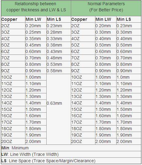
When design the board, you should consider relationship between Minimum line space (refers to Min LS later) and Minimum line width (refers to Min LW later). And to have a bigger value will make the board easier to be made.
B) Min Plated Through Hole (PTH) Diameter
PTH should be >=0.3mm; copper ring annular: 0.15mm
C) Wall copper thickness for PTH: Normal: 20um-25um, and Max 2-5OZ (50-100um).
D) Max layers: For heavy copper, max layers we can make is 20L.
Board thickness should be >1.6mm for 30OZ copper.
Impedance control, high Tg, are not workable for heavy copper.
Min Via: 0.3mm.
E) Max board size: 550x350mm is the most economical. Bigger size (550x500mm) also workable but cost will be much higher.
If you would like to know more information about heavy copper PCB (heavy copper printed circuit board) or know the questions for heavy copper PCB (heavy copper printed circuit board) in order to avoid mistakes when you design heavy copper PCB (heavy copper printed circuit board),you can visit other pages on our website or contact us for help directly.