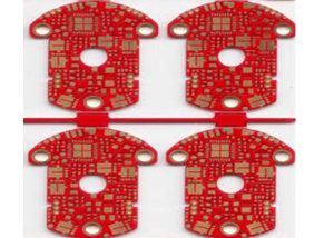
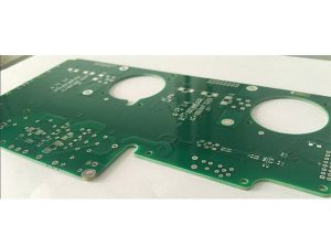
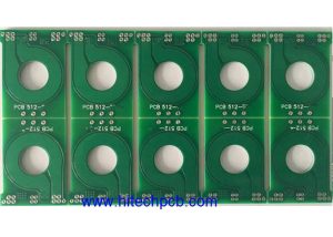
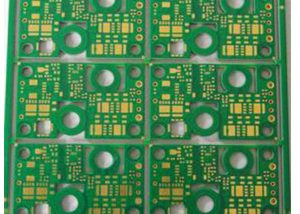
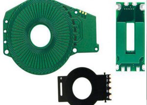
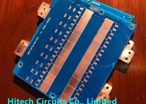
Heavy Copper PCB
Heavy copper pcb manufacturering up to 26 OZ
Hitech is a professional heavy copper pcb, thick copper pcb board manufacturer, PCB power supplier from China, we have been associated with heavy copper pcb plating since 2000 and we have won good reputation in this industry. If you have customized heavy copper pcb needs, please don’t heisitate to conatct [email protected] .
What is heavy copper PCB board
Heavy copper PCB boards ( also being called thick copper board, power board etc ) are usually bonded with a layer of copper foil on a glass epoxy substrate. The thickness of copper foil is usually 18μm, 35μm, 55μm and 70μm. The most commonly used copper foil thickness is 35μm. The thickness of copper foil used in China is generally 35-50μm, and there are also thinner ones such as 10μm and 18μm; and thicker ones such as 70μm. The thickness of the composite copper foil on a substrate with a thickness of 1-3mm is about 35μm; the thickness of the composite copper foil on a substrate with a thickness of less than 1mm is about 18μm, and the thickness of a composite copper foil on a substrate with a thickness of more than 5mm is about 55μm. If the thickness of the copper foil on the PCB is 35μm and the printed line width is 1mm, then for every 10mm length, its resistance value is about 5mΩ, and its inductance is about 4nH. When the di/dt of the digital integrated circuit chip on the PCB is 6mA/ns and the working current is 30mA, the resistance and inductance contained in each 10mm printed line are used to estimate the noise voltage generated by each part of the circuit to be 0.15. mV and 24mV.
Advantages of heavy copper PCB board
Heavy copper plate has the characteristics of carrying large current, reducing thermal strain, and good heat dissipation.
1. The heavy copper circuit board can carry large current
In the case of a certain line width, increasing the copper thickness is equivalent to increasing the cross-sectional area of the circuit, which can carry a larger current, so it has the characteristic of carrying a large current.
2. Heavy copper circuit boards reduce thermal strain
Copper foil has a small electrical conductivity (also called electrical resistivity ), the temperature rise is small when a large current is passed, so it can reduce the amount of heat and thereby reduce the thermal strain.
Metal “conductors” are divided into: ” silver→copper→gold→aluminum→tungsten→nickel→iron ” according to conductivity.
3. The heavy copper circuit board has good heat dissipation
Copper foil has high thermal conductivity (thermal conductivity 401W/mK), which can play an important role in improving heat dissipation performance, so it has good heat dissipation;
Thermal conductivity refers to the heat transfer through an area of 1 square meter within 1H for a 1 meter thick material with a temperature difference of 1°C on both sides under stable heat transfer conditions, measured by W/m·K.
Disadvantages of heavy copper PCB board
The outer copper-clad plane must be separated by the surface components and signal lines. If there is a poorly grounded copper foil (especially the thin and long copper), it will become an antenna and cause EMI problems.
If the pins of electronic components are fully connected with copper, it will cause the heat to dissipate too fast, and it will be difficult to desolder and rework soldering. The copper-clad plane of the outer layer must be well grounded, and more vias need to be punched to connect to the main ground plane. If more vias are punched, it will inevitably affect the wiring channels, unless buried blind vias are used.
Applications of heavy copper PCB board
The application field and demand for thick copper plates have been rapidly expanded in recent years, and it has become a “hot” PCB variety with good market development prospects.
The vast majority of heavy copper PCBs are high-current substrates (current x voltage = power). The main application areas of high-current PCBs are two major areas: power modules and automotive electronic components. Some of its main terminal electronic product fields are the same as conventional PCBs (such as portable electronic products, network products, base station equipment, etc.), and some are different from conventional PCB fields, such as automobiles, industrial controls, and power modules.
High-current PCBs are different from conventional PCBs in terms of efficacy. The main function of a conventional PCB is to form a wire for transmitting information. The high-current PCB has a large current through it, and the main function of the substrate carrying the power device is to protect the current carrying capacity and stabilize the power supply. The development trend of such high-current PCB is to carry larger currents, and the heat emitted by larger devices needs to be dissipated. Therefore, the large currents passing through them are getting larger and larger, and the thickness of all the copper foils of the PCBs is getting thicker and thicker. The 6 oz copper thickness of the high-current PCBs manufactured now has become normal;
The application areas of heavy copper circuit boards include: mobile phones, microwaves, aerospace, satellite communications, network base stations, hybrid integrated circuits, power supply high-power circuits and other high-tech fields.
FAQs about Heavy Copper PCBs from HiTech Circuits
1. Can HiTech Circuits customize Heavy Copper PCBs according to specific requirements?
Yes, HiTech Circuits offers custom Heavy Copper PCB fabrication to meet your specific design requirements, including varying copper thickness, board dimensions, layers, and other specifications. Our engineering team works closely with clients to ensure the final product meets their needs.
2. What quality standards do HiTech Circuits’ Heavy Copper PCBs meet?
HiTech Circuits adheres to stringent quality standards, including ISO 9001, UL certification, and compliance with IPC standards for PCB manufacturing. This ensures that all our PCBs, including Heavy Copper PCBs, are manufactured to the highest quality and reliability standards.
3. How does the increased copper thickness affect the PCB manufacturing process?
The increased copper thickness requires adjustments in the PCB manufacturing process, such as modified etching and plating techniques, to ensure precision and quality. HiTech Circuits has the expertise and equipment to handle these adjustments, ensuring the high quality of our Heavy Copper PCBs.
4. Are there any design considerations I should be aware of when designing a Heavy Copper PCB?
Yes, when designing a Heavy Copper PCB, considerations include managing the increased weight and thermal expansion, ensuring proper clearance and isolation for high-current paths, and optimizing layout for thermal management. HiTech Circuits can provide guidance on these considerations to ensure the success of your PCB design.
5. What lead times can I expect for Heavy Copper PCB production?
Lead times can vary depending on the complexity and specifications of your Heavy Copper PCB order. However, HiTech Circuits is committed to providing quick turnaround times without compromising on quality. Contact us with your specific requirements for a more accurate lead time estimate.
6. Can HiTech Circuits assist with PCB design and layout for Heavy Copper PCBs?
Yes, our team of experienced PCB designers can assist with PCB design and layout services for Heavy Copper PCBs, ensuring that your PCBs are optimized for manufacturing and meet your application requirements.
7. How can I get a quote for Heavy Copper PCB manufacturing?
To get a quote, please submit your PCB specifications and design files through our quote request form or email. Our team will review your requirements and provide you with a detailed quote as quickly as possible.