The Most Complete Knowledge about PCB (2) – Classification
As a famous Chinese PCB product supplier, Hitech Circuits Co., Limited provides premium quality Double Sided PCB, Multilayer PCB, High Density Interconnect PCB, Aluminum based PCB︱MPCB, Heavy Copper PCB, Flexible PCB︱FPCB, Rigid-Flex PCB, PCB Assembly︱PCBA, High frequency PCB. Last time, we introduce the Definition of PCB to customers. Today we will share the knowledge about the classification of PCB.
(1) Single sided PCB
Single sided board means the conductor pattern appears only on one side. Because single sided PCB has many strict limits. On trace design, only circuit at early stage use this kind of boards.
(2) Double sided PCB
Double sided board means the conductor patterns appear on both sides of the board. However if we use the conductor patterns on both sides, there should be proper circuit to connect two sides. The bridge between the circuits is called via. Those vias are plated with metal, such as tin, copper, gold, etc. Because the area of double sided PCB is two fold of the area of single sided, and the conductor pattern can cross with each other, so it suits to be used on more complex circuits.
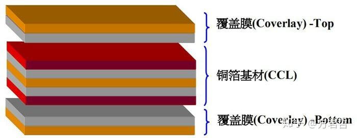
(3) Multi-layer boards
In order to enlarge the area of conductor pattern, multilayer PCB uses more single or double boards. It uses several pieces of double sided boards, and a dielectric layer is put between every layer of boards. The layers of one PCB represent the layer of conductor patterns. The amount of the layers is always even number. Technically we can make PCBs up to 100 layers.
For via, if we use it on double sided PCB, the whole boards will be drilled. While on multilayer PCB, if you just want to connect some traces, via may will waste trace space of some layers. Then we use buried vias and blind vias to solve this problem, because they are only drilled through several layers.
a. Buried vias only connect inner PCBs, so we can’t see them from the surface.
b. Blind vias connects several layers PCB with surface HDI PCB.
In multilayer PCB, the whole board directly connects the ground line and power (used for preventing affection of the transmission signals on the signal). So we divide layers into signal, power, or ground. If the components on PCB need different power supply, this kind of PCB would have more than two layers of power and wire layers.