
The most professional Chinese PCB manufacturer Hitech Circuits Co., Limited is going to share the PCB components encapsulation technology with you today.
(1) Through hole technology
It means we mount components on one side, and solder the pins on the other. The disadvantage of it is space consuming. In fact, theirs pins take up space of both sides. While the advantage of it is good construction, it can bear pressure.
(2) Surface mounted technology
it means pins are soldered on the same side as components. We don’t have to drill holes on PCB and don’t have to solder every pin. The advantage of SMT is that the components are more compact and cheaper than those in THT.
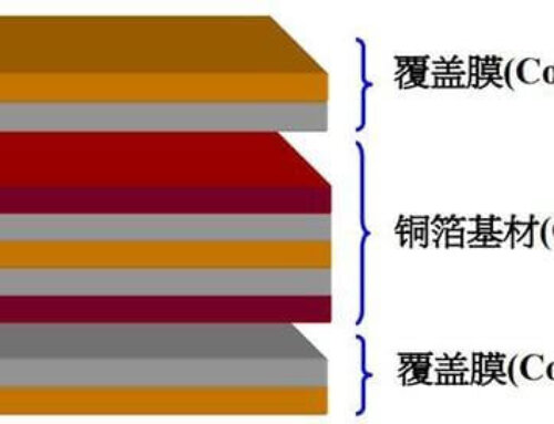
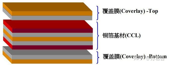
PCB Gerber files:
Usually it comprises the layout plan of signal, ground, power, solder mask, silk screen, and drilling layout plan, etc.
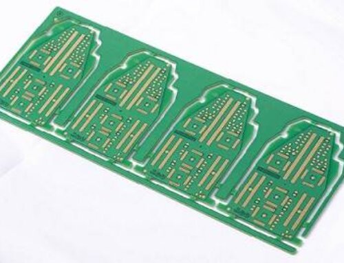
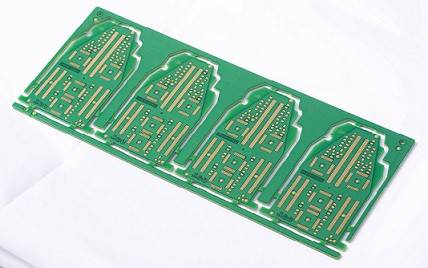
PCB Manufacture steps:
Choose base material, and then use subtractive transfer to show the artwork on metal conductor.
Established in 2007, Hitech Circuits Co., Limited has many years of experience in manufacturing PCB products, including Heavy Copper PCB, Double Sided PCB, Multilayer PCB, High Density Interconnect PCB, Aluminum based PCB︱MPCB, Flexible PCB︱FPCB, Rigid-Flex PCB, PCB Assembly︱PCBA, High frequency PCB. All our PCBs have a good reputation for high quality and reasonable price. Besides, we are a team of professional service staff, which provides the best service, before and after sales. More information, please visit www.hitechcircuits.com.