Hitech Circuits Co., Limited is a leading PCB product manufacturer in China, which provides best quality Double Sided PCB, Multilayer PCB, High Density Interconnect PCB, Aluminum based PCB︱MPCB, Heavy Copper PCB, Flexible PCB︱FPCB, Rigid-Flex PCB, PCB Assembly︱PCBA, High frequency PCB. We are willing to share knowledge about PCB with customers. Today we would like to introduce the Definition of PCB.
For standard board, it is the combination of bare board and components on it. While for bare board PCB, it is called printed wiring board. We usually call it PWB.
(1) Traces:
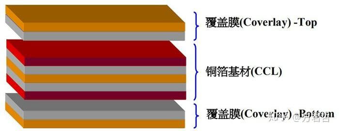
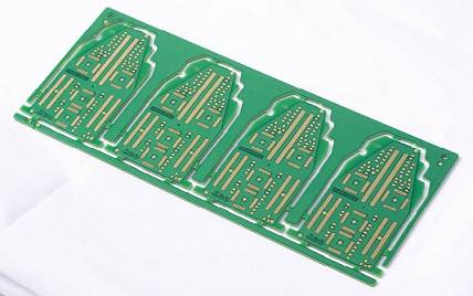
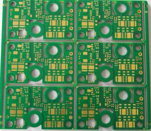
The base material of PCB is comprised of dielectric, heat insulation, uneasy to bend materials. On its surface, we can see thin traces, its material is copper. Originally the copper covered the whole PCB. Parts of it were etched during the process of production. Those parts left become net-like thin traces, which are called conductor pattern, and are used to provide circuit connection for components on PCB.
(2) Name of two side:
On most common single sided PCB, components are on one side, conductor pattern is on the other side. Then we would need to drill holes on the board, so that pins can put through the board to the other side. Therefore, the both sides of PCB are called component side and solder side.
(3) Gold finger:
Gold finger is functioned to connect two PCBs. We usually insert the gold finger of one PCB to the proper slot of the other PCB.
(4) Solder mask and silk screen:
The green or white oil on PCB is called solder mask, which is functioned as dielectric protective layer, can protects copper traces and also can prevent components to be soldered at incorrect place.
On the dielectric layer, a layer of silk screen will be printed. Some words will be printed to show the position of those components. It is also called legend. More knowledge about PCB, please visit Hitech website www.hitechcircuits.com.