Have you ever opened up an electronic device and wondered what the green board inside was? That, my friend, is called a PCB or Printed Circuit Board. It’s the backbone of nearly all electronic devices today. But, not all PCBs are created equal; some are big, complex, and incredibly fascinating. This article will take you on a journey through the world of big PCB boards, breaking down their complexities into something digestible for everyone. So, whether you’re a curious mind, a budding engineer, or just someone who appreciates the marvels of modern technology, let’s dive in together!
What Are Big PCB Boards?
Imagine you’re building a skyscraper. In the same way that a skyscraper needs a strong foundation to support its structure, electronic devices need a solid base for their components. That’s where big PCB boards come in. Unlike their smaller counterparts, big PCB boards are designed to support more complex and numerous electronic components, allowing for more sophisticated functionalities.
The Role of Big PCBs in Modern Technology
Big PCB boards are not just larger; they’re the workhorses behind the scenes. From powering the servers that run the internet to enabling the functionalities of medical imaging devices, they play a crucial role in our digital world.
Designing Big PCB Boards: An Overview
Designing a big PCB is like planning a city. You need to consider the placement of components (buildings), ensure there are pathways for electrical signals (roads), and account for power distribution (water and power lines). This complexity requires precision and foresight.
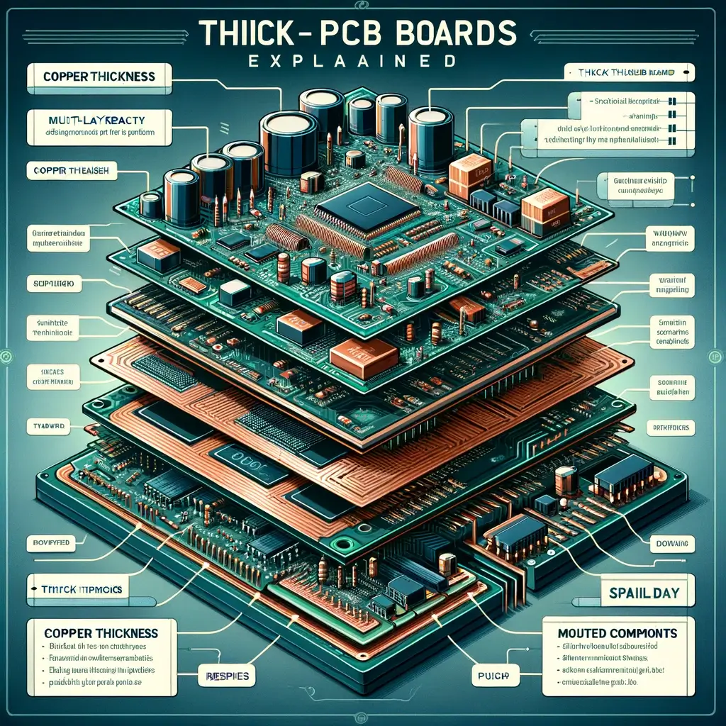
Materials Used in Big PCB Boards
The materials used in big PCB boards need to be conductive, durable, and sometimes flexible. Common materials include FR4, a fiberglass composite, for its balance of cost and performance, and newer materials like polyimide for flexibility.
Manufacturing Process
Manufacturing big PCB boards is a dance of precision and timing. It involves layering materials, etching circuit patterns, and applying a solder mask. This process requires meticulous attention to detail to ensure functionality and reliability.
Applications of Big PCB Boards
Big PCB boards are everywhere. They’re in your computer, in the control systems of airplanes, and even in the large digital billboards you see on highways. Their versatility and capability make them indispensable in the electronics industry.
Challenges in Big PCB Board Design
The larger the PCB, the more challenges arise. These include managing heat, ensuring signal integrity, and dealing with the physical constraints of larger boards. Overcoming these challenges requires innovative design and materials.
Future Trends in Big PCB Board Technology
As technology evolves, so do big PCB boards. We’re seeing trends towards more sustainable materials, flexible PCBs that can bend and fold, and even PCBs that can dissolve in water after their lifespan.
Tips for DIY Big PCB Board Projects
If you’re venturing into DIY projects involving big PCB boards, start simple. Understand the basics of electronics, experiment with design software, and don’t be afraid to make mistakes. Every failure is a step towards mastery.
Conclusion
Big PCB boards might seem daunting at first, but they are a testament to human ingenuity and the endless pursuit of advancement. They are the unsung heroes of the electronics world, enabling the complex devices that make modern life possible.
FAQs
1. What makes a PCB “big”?
A PCB is considered “big” when its size or complexity exceeds that of standard boards, usually due to the need to accommodate more components or provide more advanced functionalities.
2. How do big PCB boards manage heat?
Big PCB boards manage heat through various methods, including the use of heat sinks, thermal vias, and materials designed to dissipate heat efficiently.
3. Are big PCB boards recyclable?
Yes, many components of big PCB boards are recyclable. However, the recycling process is complex and requires specialized facilities.
4. What is the future of big PCB board technology?
The future of big PCB board technology is likely to see advancements in materials science, manufacturing processes, and design software, leading to even more powerful and efficient electronic devices.