The Internet of Things (IoT) has revolutionized how we interact with the world around us, offering unparalleled connectivity and intelligence to everyday objects. At the heart of this technological marvel lies the Printed Circuit Board (PCB), a crucial component that facilitates the seamless integration of hardware and software to bring IoT devices to life. This article delves into the fascinating world of IoT PCB assembly, shedding light on its significance, challenges, and the future direction of this dynamic field.
Understanding IoT and Its Impact
What is IoT?
IoT refers to the interconnected network of physical devices, vehicles, home appliances, and other items embedded with electronics, software, sensors, actuators, and connectivity, enabling these objects to connect and exchange data. This interconnectedness allows for more direct integration of the physical world into computer-based systems, resulting in improved efficiency, accuracy, and economic benefit.

The Importance of IoT
IoT’s impact is profound, offering new opportunities for direct integration of the physical world into digital systems, enhancing efficiency, accuracy, and economic benefits across industries. From smart homes and healthcare to agriculture and manufacturing, IoT is paving the way for a smarter, more connected world.
The Role of PCBs in IoT Devices
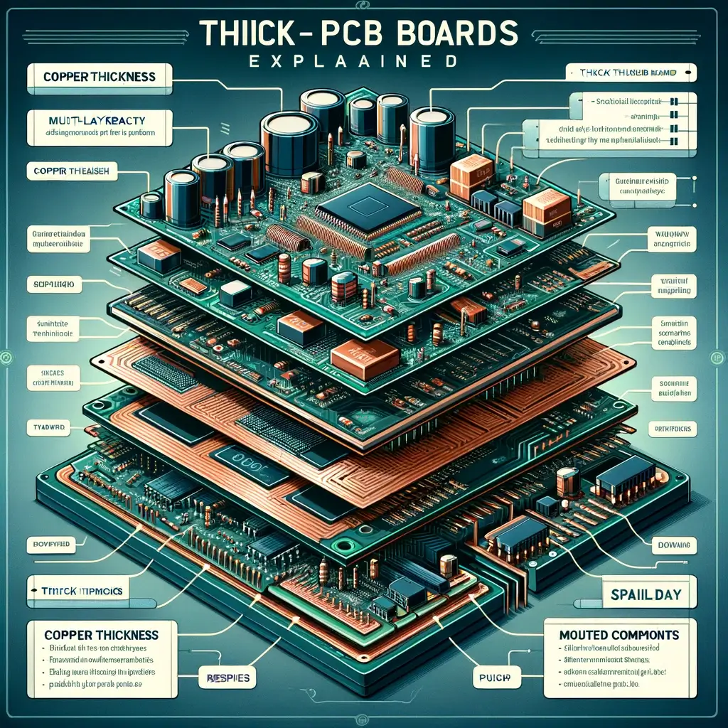
Basics of PCB Design
PCB design is foundational to IoT device functionality, providing the necessary circuitry and platform for electronic components to communicate. It involves the careful placement of components and routing of electrical signals through multiple layers of material to create a fully functional electronic circuit.
Why PCBs Are Crucial for IoT
PCBs are the backbone of IoT devices, offering the structural base that supports and connects all electronic components. They enable the miniaturization of devices while ensuring robustness and reliability, critical for the demanding environments IoT devices often operate in.
Key Considerations in IoT PCB Assembly
Design Complexity
IoT PCBs often require complex designs to accommodate a wide range of functionalities within a compact form factor, demanding high precision and expertise in PCB assembly processes.
Material Selection
The choice of materials for IoT PCBs is critical, influencing the board’s durability, flexibility, and thermal management capabilities. Advanced materials such as high-frequency laminates are often used to meet the stringent requirements of IoT applications.
Connectivity Requirements
IoT devices must support various connectivity options, including Wi-Fi, Bluetooth, and cellular networks, necessitating specialized PCB designs to accommodate these technologies.
Challenges in IoT PCB Assembly
Miniaturization
As IoT devices become smaller, fitting all necessary components on a single PCB becomes increasingly challenging, requiring innovative assembly techniques and miniaturized components.
Heat Management
Efficient heat dissipation is crucial for maintaining the performance and longevity of IoT devices, posing a significant challenge in the compact designs of IoT PCBs.
Durability and Reliability
IoT devices often operate in harsh environments, demanding PCBs that are not only compact and efficient but also durable and reliable.
Future Trends in IoT PCB Assembly
Advancements in Materials
Emerging materials offer enhanced performance and durability for IoT PCBs, paving the way for more robust and efficient devices.
Integration of AI and ML
The integration of Artificial Intelligence (AI) and Machine Learning (ML) into IoT devices is expected to further enhance their capabilities, requiring more advanced PCB designs to support these technologies.
Conclusion
IoT PCB assembly is a critical component of the IoT ecosystem, enabling the seamless operation and connectivity of devices that make our lives smarter and more convenient. Despite the challenges, advancements in technology and materials continue to push the boundaries of what’s possible, promising an exciting future for IoT PCB assembly.
FAQs
What is IoT PCB Assembly?
IoT PCB Assembly refers to the process of assembling electronic components onto a PCB to create a functional IoT device.
How do PCBs impact the functionality of IoT devices?
PCBs are fundamental to IoT devices, providing the necessary circuitry for component communication and functionality within a compact, efficient design.
What are the main challenges in IoT PCB assembly?
Challenges include miniaturization, heat management, and ensuring durability and reliability in harsh environments.
What future trends are emerging in IoT PCB assembly?
Emerging trends include the use of advanced materials and the integration of AI and ML into IoT devices for enhanced capabilities.
How can one ensure the durability of IoT PCBs?
Selecting appropriate materials, designing for environmental conditions, and incorporating advanced manufacturing techniques are key to ensuring the durability of IoT PCBs.