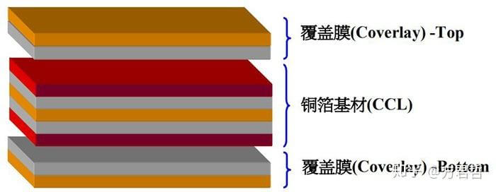
Thicken the copper plating is mainly designed to make sufficient thickness of copper coating in the hole so as to ensure that the value of resistance in the range of technical requirements. As the insert, the hole is a fixing position to ensure the connection strength; as the device used for surface encapsulation, some are only used as the conducting holes, which play the role of the two sides’ electric conduction. Before electroplating the heavy copper PCB, the following items should be checked:
1. Check the main quality of hole metallization, it should be guaranteed that the hole is without residue, burr, black holes and voids;
2. Check whether the substrate surface is dirty or has other residues;
3. Check the number, drawing number, process documentation and process instructions of the substrate;
4.Make clear of the installation location, installation requirements and the plating area the plating tank can bear;
5. Make clear of the plating area, process parameters to ensure the stability and feasibility of the plating process parameters;
6. Clean and prepare the conductive parts, first power on to make the solution of the active state;
7. Check whether the liquid component is qualified and the plate surface area status; if applied the spherical anode, the consumption also must be checked;
8. Check the fixing state of the contact area and the range of voltage and current.
More information about heavy copper PCB, please visit www.hitechcircuits.com.