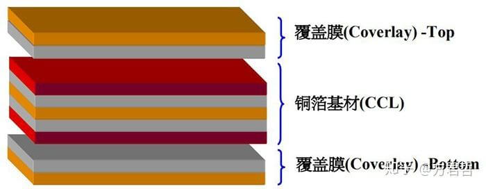
Printed Circuit Board (PCB) is a mechanical assembly consisting of layers of fiberglass sheet laminated with etched copper patterns. It is used to mount electronic parts in a rigid manner suitable for packaging. Also known as a Printed Wiring Board (PWB).
A schematic diagram must be made available that shows the connection of the parts on the board. Each part on the schematic should have a reference designator that matches the one shown on the Bill of Materials (BOM). Many schematic layout programs will allow automatic generation of the BOM.
A functional PCB is not a finished product. It will always require connections to the outside world to get power, exchange information, or display results. It will need to fit into a case or slide into a rack to perform it’s function. There may be areas that will require height restrictions on the board (such as a battery holder molded into the case or rails in a rack the board is supposed to slide into). Tooling holes and keep-out areas may be required in the board for assembly or manufacturing processes. All these outside factors need to be defined before the board can be designed, including the maximum dimensions of the board and the locations of connectors, displays, mounting brackets, or any other external features.
Generally, it is best to place parts only on the top side of the board.
First place all the components that need to be in specific locations. This includes connectors, switches, LEDs, mounting holes, heat sinks or any other item that mounts to an external location.
Give careful of thought when placing component to minimize trace lengths. Put parts next to each other that connect to each other. Doing a good job here will make laying the traces much easier.
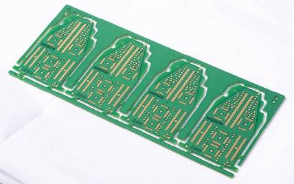
PCB fabrication
PCB Manufacturer, Advanced Circuits Quick turn Printed Circuit Boards Production, Circuit Board Fabrication, PCB’s maker and Distributor