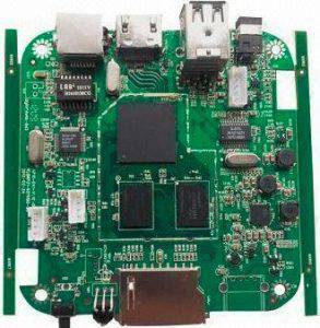
SMT PCB Assemblies are getting more and more complex. While SMT PCB Assembly makers strive for 100% yield, the fact is that achieving it is extremely difficult. While a majority of electronics today utilize SMT Components however the reduced component sizes make putting them onto PCBs extremely difficult. Other than this, there are a number of other defects that SMT metal core pcb Assembly has to overcome, primary among them include:
Poor Solder Paste Release
Solder Paste Release, in turn, is determined by aspect ratio and surface area ratio. Aspect ratio compares the smallest dimension of the stencil aperture to the stencil foil thickness. An aspect ratio of lower than 1.5 is not acceptable. Surface Area Ratio compares the surface area of the stencil aperture to the surface area of the stencil aperture walls. The lowest acceptable surface area ratio is 0.66. While the aspect ratio and surface area ratio help predict solder paste release, what is also important is the adhesion strength of the solder paste to the SMT pad, which in turn is determined by the size of the SMT Pad. Difference in surface finishes can in turn impact the SMT Pad sizes. To be able to accurately predict solder paste release a modified surface area ratio formula must be considered which takes into account changes in SMT Pad sizes on account of copper weights and surface finishes. This is gaining more and more importance as smaller components become more mainstream. Typically the bottom of the SMT Pad matches the size in the electronic PCB files while the top is smaller. It is this smaller size top that needs to be considered in calculating the stencil surface area ratio as the smaller size top has less surface area.
Bridging at Print
Besides impacting solder paste release, copper weights and surface finishes also impact bridging. Heavy copper weights or non-flat surface finishes degrade the seal between the PCB and the stencil. This can in turn allow solder paste to squeeze out during printing and also cause bridging at print. The seal is dependent on the size of the SMT Pad and stencil aperture. Stencil apertures larger than the SMT Pads can cause solder paste to squeeze out between the PCB and the stencil.
In order to circumvent this problem, a width reduction when it comes to stencil apertures is required. This is especially true of heavy copper weights and non-flat PCB surface finishes. This in turn ensures that the chances of the solder paste squeezing out between the PCB & stencil is minimized.
Insufficient Solder Volume at SMT reflow
While it is a common defect, it is typically caught only at the end of the SMT Process during visual or automated optical inspection. A DFM review sometimes can also catch the insufficient volume before production. To overcome this problem, the required volume increase is based on the size difference of the leadless termination and PCB Land pad. Also the additional solder paste volume needs to be printed to the toe side on case of leadless components. Also increasing the stencil aperture width needs to be avoided. What is also important to note is the stencil foil thickness. In cases where the foil thickness needs to be adjusted to accommodate SMT components, the stencil aperture volume also needs to be increased.
Bridging at SMT Reflow
Many a times bridging at SMT Reflow is caused due to solder paste squeezing out between the PCB & stencil at print, at others it is on account of Metal core PCB fabrication issues, placement pressure, reflow over settings etc. Bridging at SMT Reflow can also occur on account of gull wing packages as they have component lead exposed to the heating. Leadless packages, on the other hand have uniform heating. Gull wing packages also have limited amount of surface area to wet the solder. In case of too much solder, the excess can spill off on to the PCB Pad. The reduction in solder paste volume, however should always be centered on the gull wing foot and not the PCB Pad. While for most assemblies the volume reductions will reduce dramatically, care needs to be taken when the PCB Surface finish is OSP(Organic Solderability Preservatives) and the solder is lead free. In case of lead free solders volume reductions can leave OSP exposed after reflow. Exposed OSP, in turn can lead to a whole lot of issues that impact reliability.
While some SMT defects are limited to a particular assembly line or particular location, many others such as solder paste release, bridging at print, bridging at SMT Reflow, insufficient solder volume at SMT Reflow and more mentioned above are universal and are not limited to a particular set of variables. Their effects therefore need to be closely considered to ensure reliability in operations.


