In the 50+ years since printed circuits have become commonplace, the complexity and density of interconnect offered has increased markedly. For example, tracks that were 1mm wide successively became 0.25mm and 150µm, and 100µm is nowadays achievable in volume, although prudence suggests that such densities are not used for large areas. And holes, which used to be 0.9–1.2mm diameter for through-hole connectors, are now typically 0.35mm or less for vias. In other words, conventional printed circuit technology is still capable of meeting many of today’s requirements. Yet there is a grouping of products referred to as “High Density Interconnect pcb” (HDI board for short) that are used to create still denser interconnect, and it is these that are the subject of this topic paper.
Drivers for higher-density interconnection come under three headings, portability, performance and parts:
- Portability, with fast-growing markets for products such as digital cameras, MP3 players and palm computers, all of which represent new opportunities made possible by electronics becoming smaller and lighter.
- Performancewith increased processing speeds and more RF and microwave communications, at frequencies up to 40GHz in some telecoms areas.
- Parts, meeting the silicon challenge to provide more leads in a smaller footprint, which equates to more connections per unit area.
All of these drivers create a demand for denser interconnect, with smaller track and gap dimensions, smaller vias, and more buried vias. Whilst this is not necessarily accompanied by a change in board practice, conventional constructions reach their limits at the bottom end of the size range, so we need to find alternatives.
The most significant change between conventional boards and HDI PCB is in the form of the vias. As we show in Figure 1, not only do conventional through vias have sizes that are constrained by the capability of the drilling operation, but they would also normally be kept well away from solder joints in order to avoid solder wicking down the hole. In consequence, conventional assembly designs will employ some separation between components and vias, except where (expensive) buried vias are used.
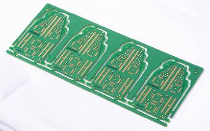
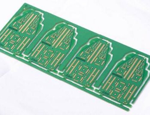
Hitech Circuits Co., Limited is a China pcb manufacturer of High Density Interconnect PCBs (HDI PCBs). Our HDI capabilities include laser microvias, blind and buried vias, fine lines and spaces, sequential lamination, via-in-pad technology. We have provided microelectronic pcbs with fine pitch devices down to 200 microns, using 50 micron laser drilled via-in-pad technology and thin build-up materials. Upload your data and receive a free consultation and review of your HDI design today or contact us if you need any design help. Experience our expertise and feel the difference.