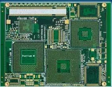
As is known to all, via is one of the important parts of multilayer PCB. The cost of drilling usually makes up 30%~40% of the cost of PCB manufacture.
Simply speaking, every hole on High Density Interconnect PCB may be called via.
Functionally, via can be divided into two types: firstly, used for electro-connection among layers; secondly, used for fixing components.
Technically, it may also be divided into three types: blind via, buried via and though hole. Blind via is located on the top and bottom surfaces of the PCB, deep and used for connection of top traces with the inner layer traces below.
Buried via is the connecting hole which is located in the inner layer of the High Density Interconnect PCB and won’t extent to the surface.
Through hole goes through the whole PCB, which is used to realize inter-connection or used as components mounting position hole. Due to the simple technique and low cost, most of PCBs use it rather than the other two via.