Do you know how to identify the plated through hole cross-section defect for high frequency PCB to keep your PCB at superior quality performance? Let PCB board supplier Hitech Circuits advise the most common quality defects in the plated through hole of the high frequency PCB.
To demonstrate the major quality defects of the plated through hole of high frequency PCB, PCB board supplier Hitech Circuits attaches a graphical representation for your better understanding:
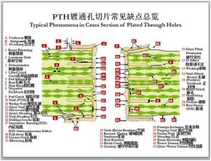
According to the above graphical representation from PCB board supplier, the major quality defects of the plated through hole of high frequency PCB include: undercut, outgrowth, overhang, resin blistering, laminate void, delamination, lifted land crack, pad lifting, burrs, pink ring, negative etch-back, copper foil crack, void plated through hole; wedge void, glass fiber void, micro-void, arrow heading, nail heading, drilling cracks, inner layer burning / interconnection defect, pull away, corner crack, blistering, voild (resist residues), burned plating, starburst, red rotation, resin crack, glass fiber crazing, glass fiber protrusion, D-effect, wicking, void (metal resist), (positive) etch-back, barrel crack, shadowing, nodule, rest smear (ICD), foreign inclusion, prepreg void, pocket void, measling, resin recession, weave texture, glass-weave texture.
This graphical representation of major quality defects of the plated through hole of high frequency PCB tells you how to identify the quality defects of the cross-section of your high frequency PCB so you can measure the impact and risk of the quality defects and ask your supplier to work out a corrective actions to get it covered and prevent damage to your assemblies.


