- Program the SMT placement machine
According to the BOM position map provided by the customer, program the coordinates of the location of the components. Then carry out the first piece with the SMT chip processing data provided by the customer.
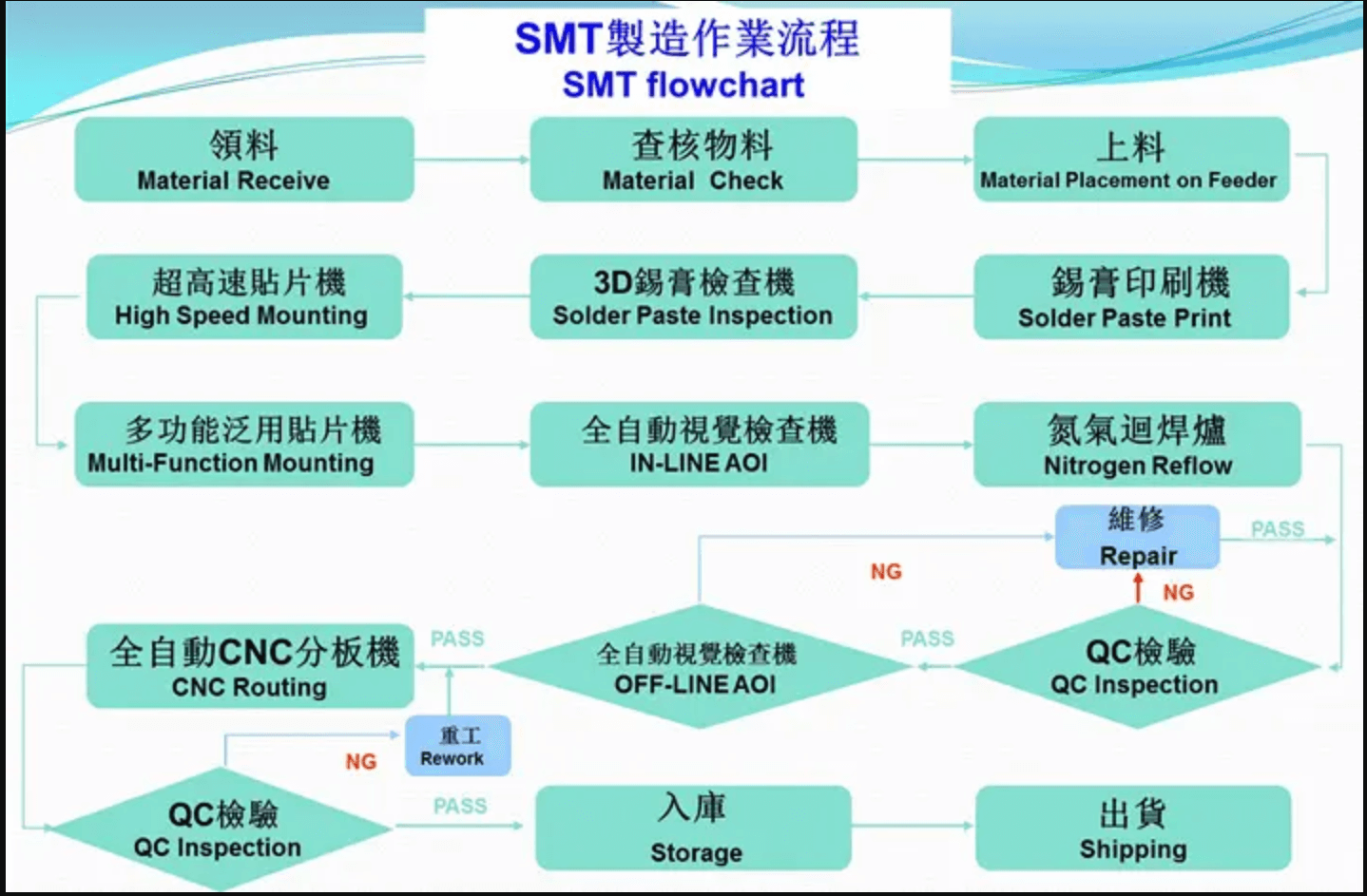
- Printing solder paste
The solder paste is stenciled to the PCB board where the electronic component SMD needs to be soldered to prepare for the soldering of the components. The equipment used is a screen printing machine (printing machine), which is located at the forefront of the SMT chip processing production line.
- SPI
Solder paste detector, detects whether the solder paste printing is a good product, whether there is less tin, leaking tin, more tin and other undesirable phenomena.
4.SMT
Accurately install the electronic components SMD on the fixed position of the PCB. The equipment used is a placement machine, which is located behind the screen printing machine in the SMT production line.
The placement machine is divided into high-speed machine and general-purpose machine.
High-speed machine: used to paste components with large pin spacing and small pin spacing
Universal machine: paste small pin pitch (pin density), bulky components.
- High temperature solder paste melting
Mainly, the solder paste is melted at high temperature, and after cooling, the electronic components SMD and the PCB board are firmly welded together. The equipment used is a reflow soldering furnace, which is located behind the placement machine in the SMT production line.
- AOI
Automatic optical detector to detect whether the soldered PCBA components have poor soldering, such as tombstone, displacement, empty soldering, etc.
- Visual inspection
The key items of manual inspection and inspection: whether the PCBA version is the changed version; whether the customer requires components to use substitute materials or components of designated brands and brands; IC, diodes, triodes, tantalum capacitors, aluminum capacitors, switches, etc. Whether the direction of the directional components is correct; defects after welding: short circuit, open circuit, fake parts, fake welding.
- Packaging
Products that have passed the test will be packaged separately. The commonly used packaging materials are anti-static bubble bags, electrostatic cotton, and blister trays. There are two main packaging methods, one is to use anti-static bubble bags or electrostatic cotton into rolls, which are the most commonly used packaging methods at present; the other is to customize blister trays according to the size of PCBA. Put it in a blister tray and unpack it, mainly for PCBA boards that are sensitive and have vulnerable patch components.
Main equipment for PCBA production
Solder Paste Printer, SPI Solder Paste Printing Inspection Machine, Mounter, Reflow Soldering, Furnace Temperature Tester, AOI Inspection Machine, Component Foot Cutting Machine, Wave Soldering, Soldering Furnace, Board Washer, ICT Test Fixture, FCT Test fixtures, aging test racks, etc., stencil cleaning machines, X-ray inspection machines, and PCBA processing plants of different scales will be equipped with different equipment.


