Printed Circuit Board or PCB’s are an integral part of every electronic device. They are the green chips that you can find within all electronic devices. These green chips or Printed Circuit Boards are printed with copper lines called traces, which carry signals to various components. This systematic transmission of signals ensures the proper functioning of the electronic device.
PCBs are omnipresent in every modern day electronic device. As the technology advances and the electronic devices becoming more and more compact, there is a drastic reduction in the size of the PCB. This reduction in size increases the complexity of a PCB. A complex PCB must undergo a complex manufacturing procedure and various levels of assembly.
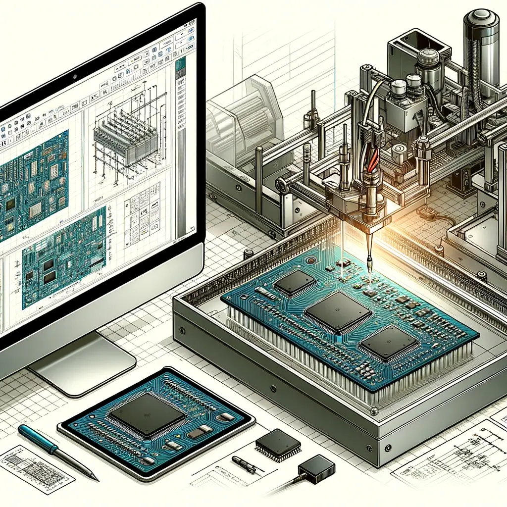
The following are the various steps involved in the present day PCB assembly process.
Solder Paste Stenciling: -This is the initial step in PCB assembly, in this step solder paste is applied to the PCB. A thin steel stencil that allows the placement of solder paste in certain areas is placed on the PCB. Components will be placed in the certain places where the solder paste is applied. The solder paste is a greyish material of metallic components.
Pick and Place: -Following the solder paste stencilling is the Pick and Place. As the name suggests the Pick and Place step is where the components are placed on the PCBs. This step of the assembly process started out as a manual procedure. However, in recent times this step is automated for increased efficiency and accuracy.
Reflow Soldering: – Once the PNP machine places the components on the PCB, the placed components need to be soldered. In the current day PCB assembly process, PCB manufacturers employ the process called Reflow Soldering. During Reflow Soldering, the PCBs that have the stencilled solder and component placed are made to go through a conveyor belt that goes through a Reflow Oven. In the oven, the PCBs are heated to a temperature of 250 degree Celsius. This heat enables the solder paste to melt and merge with the placed components. Following which, the heated PCB’s are moved through cooler heaters, which solidifies the melted solder creating a permanent joint with the PCB and the components.
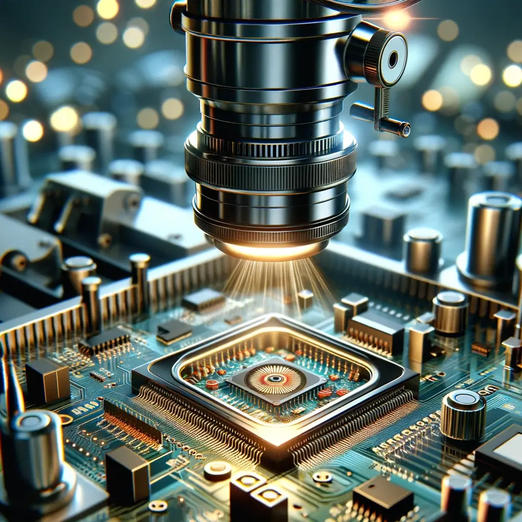
Inspection and Quality Control: – After the Reflow soldering the each PCB is tested for functionality. The movement during the previous assembly procedures may slightly move the placed component, these slight deviation results in shorts. So, the PCB is checked for any such misalignments. This process used to be manually checked. However, with increased accuracy requirement nowadays, professional PCB manufacturers employ the automated machine testing process called the Automatic Optical Inspection. More complex or layer PCBs undergo X-ray inspection to identify any hidden imperfections or errors.
Through Hole Component Insertion: – Apart from SMD or surface mount components, PCBs may require Plated Through Hole component, also called as PTH components. Soldering paste is not suitable for PTH components. Therefore, PCB manufacturers employ Manual Soldering or Wave Soldering for PTH components.
Final Inspection and Functionality Test: – The given steps conclude the assembly procedure. However, no finished product is approved for consumers until it passes the final inspection and functional test. This is a straightforward test that stimulates the PCB to operate in a normal circumstance. The approved PCBs are the fully assembled functioning product.


