Today's Top Stories
Health News
View All
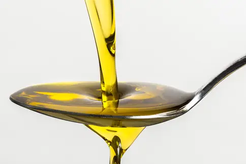
Olive Oil May Lower Your Risk of Dementia-Related Death
New research shows that consuming about half a tablespoon of olive oil a day was linked to a lower risk for dementia-related death.
Vegans and Vegetarians Sleep More Minutes Per Night: Survey
Teen Mental Health Crisis Deepens
Postpartum PTSD: Right Diagnosis Can Help Mothers and Babies
Special Section
 Content on Myasthenia Gravis
Creating a Plan for Your Treatment and Well-Being
Find out how to build a treatment plan with your doctor plus how to manage your overall health while living with myasthenia gravis.
 Spotlight on a Clean Home
How Clean Is Your House?
Learn how to beat germs and improve air quality in every room of your home.
 Spotlight on Medicare Advantage
Discover How You Can Make the Most of Medicare Advantage
From making your prior authorization process easier to understanding your prescription coverage, what to know.
Free WebMD Newsletters
Doctor-approved health and wellness information delivered to your inbox.

Patient and Expert Contributors
View All- Substance Abuse & Addiction
 Ashley WalkerDiagnosed since 2010
 - Brain & Nervous System
 Ashley BrooksDiagnosed since 2017
 - Pain Management
 Anita Gupta, PharmD, DOBoard-certified anesthesiologist and pain management physician
 - Digestive Problems
 Suzie FinkelRegistered dietitian
Health A - Z
View AllADD/ADHD - Childhood
ADHD
Allergies
Alzheimer's
Ankylosing Spondylitis
Anxiety Disorders
Arthritis
Asthma
Back Pain
Cancer
Children's Vaccines
Cholesterol
Cold, Flu, & Cough
COPD
Coronavirus
Depression
Diabetes
Digestive Disorders
Eye Health
Health & Balance
Heart Health
Heartburn/GERD
Hypertension
Lung Cancer
Mental Health
Migraines
Multiple Myeloma
Multiple Sclerosis
Oral Care
Orthopedics
Osteoporosis
Ovarian Cancer
Prostate Cancer
Psoriasis
Rheumatoid Arthritis
Schizophrenia
Sexual Conditions
Skin Problems
Sleep Disorders

Our Content Is Different Because We Set the Bar Higher
As a leader in digital health publishing for more than 25 years, WebMD strives to maintain the most comprehensive and reliable source of health and medical information on the internet.
We recognize the responsibility that comes along with being the most well-known and trusted health information platform — and we take that responsibility seriously by:
- 01Charging our content creators to practice journalistic principles of excellence and provide objective, accurate, and balanced reporting
- 02Maintaining editorial independence and transparency into how we protect the integrity of our content
- 03Regularly reviewing and updating our content by working with our network of more than 100 doctors and health experts


