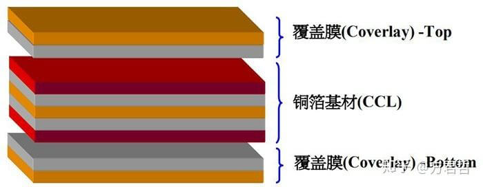
High Density Interconnect or HDI boards are already one of the fastest growing technologies in PCB as it contains of blind and buried vias with microvias of.006 or less in diameter. They have a higher circuitry density than traditional circuit boards. Specialty equipment and trained technicians follow the process closely to achieve the perfect hidden via.
You can find 6 different types of HDI boards:
- Through vias from surface to surface
- With buried vias and through vias
- Two or more hdi layer with through vias
- Passive substrate with no electrical connection
- Coreless construction using layer pairs
- Alternate constructions of coreless constructions using layer pairs
Printed circuit board using HDI technology is a thorough consumer driven technology and they are proving that bigger is not always better. The via-in-pad process supports more technology on fewer layers. Since the late 1980’s we have seen various gadgets like mobile phone, video cameras and laptop have shrink to fit in the palm of your hand but yet stay very much efficient and much more than the earlier times. In such a scenario, High Density Interconnect PCB has helped in the development of transformations where the products do more, weigh less and are physically smaller.
HDI technology is growing so fast that already the designers have the option to place more components on both sides of the raw PCB. Multiple via processes including via-in-pad and blind via technology is allowing designers more PCB real estate to place components in a tighter space. The designs which are developing in PCBs are now faster for transmission of signals and theya re playing a crucial role in the reduction of signal loss and crossing delays.

The via-in-pad process is allowing vias to be placed within the surface of the flat lands. The via is plated and filled with either conductive or non-conductive epoxy then capped and plated over, making it virtually invisible. Since there are various via fill materials like non conductive epoxy, conductive epoxy, copper filled, silver filled and electrochemical plating, there is lots of scope. Vias and microvias are drilled, blind or buried, filled then plated and hidden beneath SMT lands.
Processing vias of this type requires specialty equipment, mini-components and thinner materials which allows electronics to shrink in size while expanding technology, quality and speed. Mobile computing and working from home pushed technology further to make computers faster and lighter, allowing the consumer to work remotely from anywhere.
Apart from all the amazing development quality remains the most important factor for consumer to buy the service. Using High Density Interconnect technology during design, it is possible to reduce an 8 layer through-hole PCB to a 4 layer HDI microvia technology packed PCB. Although the microvia process increases the cost of the HDI PCB but a proper design and reduction in layer count reduces cost in material square inches and layer count more significantly.