One of several methods accustomed to boost electrical circuit density in printed wiring board (PWB) would be to use blind together with buried vias. If you do not wish to fully extend through the printed board, blind and buried vias will serve the purpose and additionally go only partly via between the multilayer circuits, joining just the internal layers that require relationship.
 Thanks to these vias don’t proceed through the complete multilayer board, the supply concerning spot within the other layers turns into beneficial for additional circuit routing. The expression buried vias are those who usually are not seen in the outside connected with the fabricated printed wiring board, and additionally are formed in the sub-composite or copper-clad laminate. Blind vias are the ones that are visible from your exterior connected with the HDI pcb display board but tend not to go completely throughout the total board.
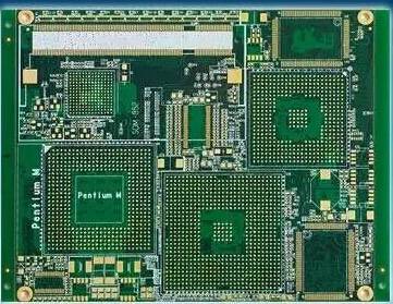
By using the size related with these small vias, this significantly elevated interconnection density related with a board. Microvia or high-density interconnection (HDI) printed wiring board makes use of these technologies to increase circuit density; case in point is cell mobile phone that is certainly utilizing microvia engineering because of on the request for scaled-down packaging devises. The processes accustomed to sort microvias contain laser ablation, plasma etching, plus photoimaging.
Printed wiring boardContent employed in High Density Interconnect PCB supplier designs utilizes an natural and organic reinforcement that could be laserablated or plasma-etched. The vastly use organic reinforcement materials is aramid fiber-based. The aramid fibers are shaped right into a sheet that’s impregnated together with the resin method. With this method, the two copper-clad laminates and then prepregs could be manufactured and also used in multilayer board purposes.


