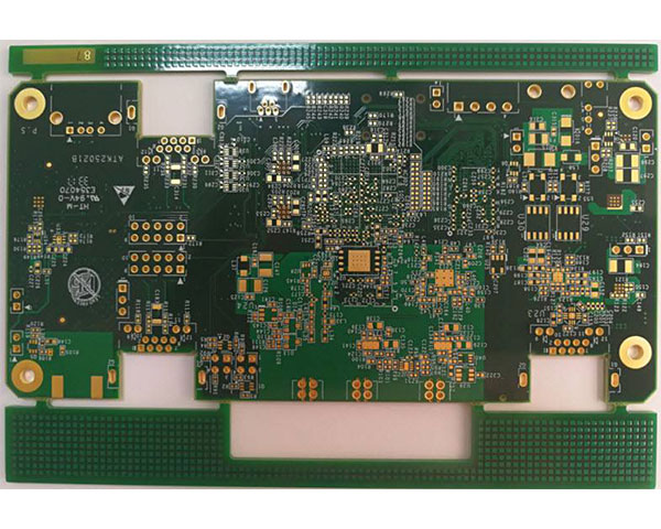
Project Description
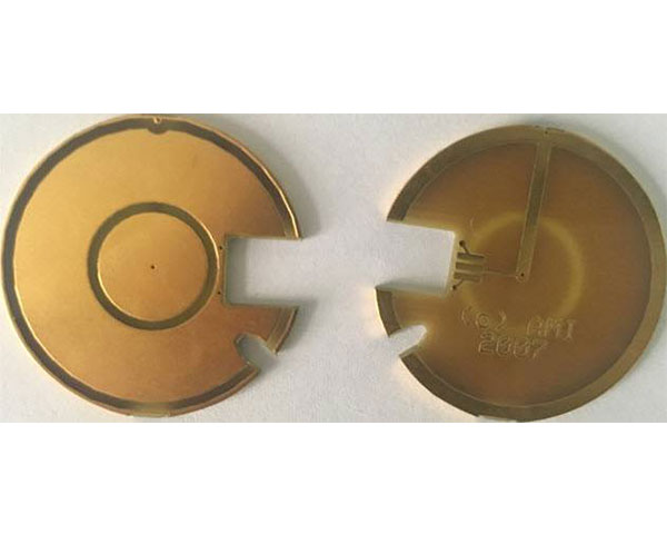
Double layers transparent PCB
The surface of the double-layer transparent pcb board is flush with the upper surface of the conductive circuit, the surface of the entire high-conductivity transparent glass-based circuit board is smooth, the conductive circuit is not easy to be damaged, and the conduction ability is strong. It is widely used in computers and peripheral auxiliary systems, medical equipment, mobile phones, digital (camera) cameras, communication equipment, precision instruments, aerospace, etc.

Technical Parameters
- Material: FR-4 Tg135
- PCB Size:158.75*118.6mm
- Board thickness: 1.6mm
- Surface finished: HAL LF
- Copper thickness: 1/1 Oz
- Min through hole: 0.2mm
- Consumer Electronics